
Blast away defects with lasers
KNOXVILLE, TN, October 06, 2023 /24-7PressRelease/ — A new laser-based process chain has been developed to fabricate fused silica optics. It uses a CO2 laser to ablate the surface of the optics for the precise removal of subsurface mechanical damage. The results show that the laser-induced damage thresholds of samples fabricated using the new process are significantly higher than those using conventional methods. This represents a promising direction for manufacturing highly damage-resistant fused silica optics for high-energy laser applications.
Residual processing defects significantly reduce fused silica optics’ laser-induced damage threshold (LIDT), which seriously limits their performance and lifetime in high-energy laser applications. Extensive research has been conducted to eliminate and suppress these defects, but manufacturing fused silica optics with a high LIDT remains a bottleneck problem.
A new laser-based process chain has been developed in a new paper published in Light: Advanced Manufacturing. The scientists, led by Professor Chaoyang Wei and Jianda Shao, can now fabricate fused silica optics with high LIDTs. The process uses a CO2 laser to ablate the optic’s surface in a uniform layer-by-layer fashion, which allows for the precise removal of subsurface mechanical damage and surface/subsurface contamination. The results show that the LIDTs of samples fabricated using the new process chain are significantly higher than those manufactured using conventional methods. This new process represents a promising new direction for fabricating highly damage-resistant fused silica optics for high-energy laser applications.
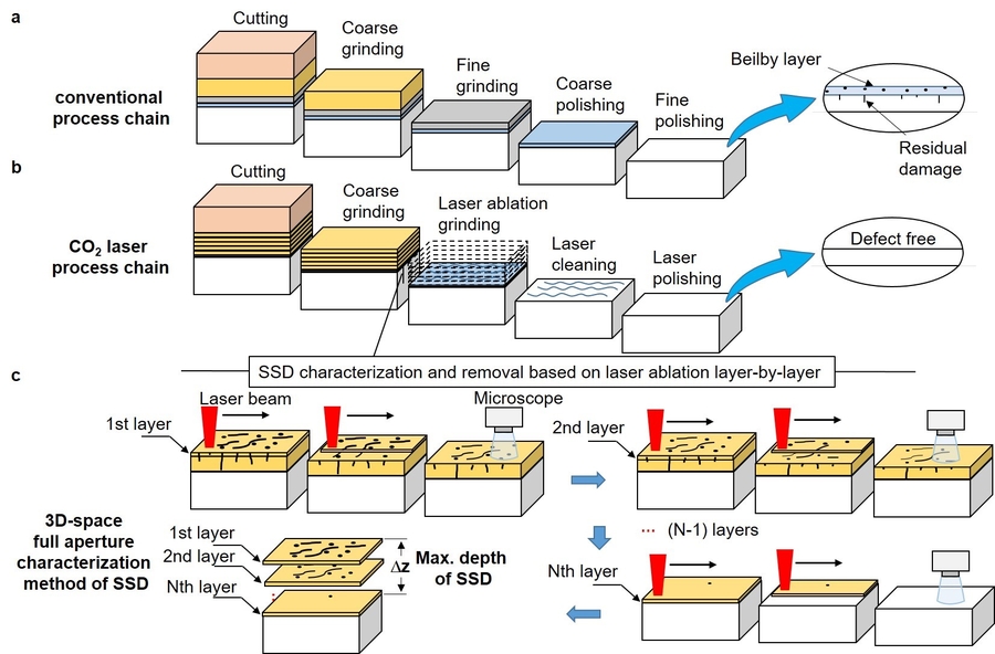
Residual processing defects significantly reduce the LIDT of fused silica optics, which seriously limits their performance and lifetime in high-energy laser applications. Conventional processing methods have focused on effectively managing subsurface mechanical damage (SSD) during grinding, but this is not always successful. Additionally, conventional polishing methods can lead to polishing contaminants. Postprocessing techniques such as HF-based etching have been developed to eliminate contaminants and SSD, but these techniques can also introduce new defects.
To further improve the damage resistance of fused silica surfaces, new methods must be developed to address the 3D-space full-aperture characterization of SSD and the introduction of new defects in the postprocessing step.
One promising new method is laser radiation processing of fused silica glass. Since the nature of non-contact and no need for polishing slurry, laser processing has a natural advantage in suppressing defect introduction. A CO2 laser can be used to ablate the optic’s surface in a uniform layer-by-layer fashion, which allows for the precise removal of SSD and surface/subsurface contamination.
A CO2 laser process chain has been proposed for manufacturing highly damage-resistant fused silica optics. The process chain includes laser ablation, laser cleaning, and laser melt polishing. First, theoretical and experimental research verified the feasibility of characterizing SSD based on uniform layer-by-layer laser ablation. The SSD characterization method was coupled with the laser ablation grinding process to achieve complete SSD removal. Next, a laser conformal cleaning method was proposed to effectively remove ablation contaminants. Finally, with laser melt polishing, suppression of damaged precursors was realized in the entire process chain, and a fused silica sample with a high LIDT was obtained.
The proposed characterization method provides a new tool for guiding the optimization of finishing processes. This new processing strategy offers a new approach to low-defect manufacturing of fused silica optics.
References
DOI
10.37188/lam.2023.021
Original Source URL
https://doi.org/10.37188/lam.2023.021
Funding information
This work was supported by the National Key Research and Development Project, Shanghai Sailing Program, National Natural Science Youth Foundation of China, Natural Science Foundation of Shanghai, Key Projects of the Joint Fund for Astronomy of the National Natural Science Funding of China, and the Youth Innovation Promotion Association of the Chinese Academy of Sciences.
Contact
Chaoyang Wei
Precision Optical Manufacturing and Testing Centre, Shanghai Institute of Optics and Fine Mechanics, Chinese Academy of Sciences, Shanghai, China, 201800, [email protected]
About Light: Advanced Manufacturing
Light: Advanced Manufacturing (LAM) is a new, highly selective, open-access, and free-of-charge international sister journal of the Nature Journal Light: Science & Applications. The journal aims to publish innovative research in all modern areas of preferred light-based manufacturing, including fundamental and applied research as well as industrial innovations.
Chuanlink Innovations, where revolutionary ideas meet their true potential. Our name, rooted in the essence of transmission and connection, reflects our commitment to fostering innovation and facilitating the journey of ideas from inception to realization.
Related Link:
http://chuanlink-innovations.com
—
For the original version of this press release, please visit 24-7PressRelease.com here